
Chip process node (3 nm, 4 nm): what the nanometres mean
A process node is the generation of technology used to make a chip. It is labelled in nanometres (nm): 7 nm, 4 nm, 3 nm. A smaller number usually means smaller transistors, more computing blocks in the same area and lower power consumption.

In plain words
Imagine writing on a sheet of paper. The finer the pen, the more words fit on the page. The process node is like the thickness of the "pen" used to draw billions of transistors on silicon. A finer "pen" means more transistors in the same chip - and so more power and less heat.
How it works
- A chip is made of billions of transistors - microscopic switches.
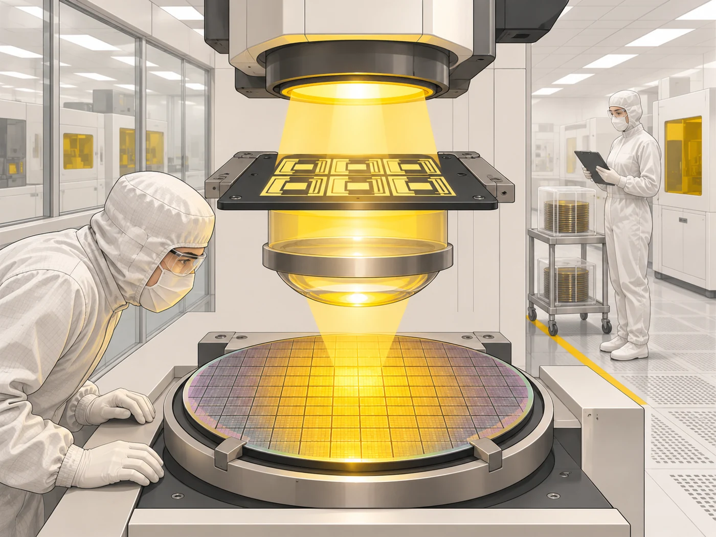
- They are "printed" onto a silicon wafer with light through masks, layer by layer.
- A new process node allows smaller, more densely packed transistors.
- Smaller transistors switch using less energy.
- Only a few companies make the most advanced chips; the best known are TSMC and Samsung.
Where you'll see it
The process node appears in the specs of smartphone, tablet and laptop processors: "3 nm", "4 nm", "TSMC N3E". In our comparisons it shows up in chip descriptions. Flagship chips are now made on 3 nm processes, mid-range on 4-6 nm and budget on 6-12 nm.
Does it matter when buying
Yes, but as part of the picture. A chip on a newer node usually runs cooler and lasts longer on a charge. Still, I do not recommend comparing nanometres alone: core architecture and optimisation matter just as much. It is better to look at the specific chip name and battery life tests.
Myths
- Myth: 3 nm is the real size of a transistor. Reality: Today the nanometres are more a marketing name for a generation than the exact size of any part.
- Myth: The same nm from different factories means the same quality. Reality: Process nodes from different manufacturers with the same number can differ noticeably.
FAQ
Why is a smaller node better?
More transistors per area and less energy per operation.
What is TSMC?
A Taiwanese company and the largest contract chipmaker, producing chips for Apple, Qualcomm, MediaTek and others.
Will there be nodes smaller than 1 nm?
Manufacturers are already moving to labels like "2 nm" and "18A", and beyond that to new types of transistors.
Related terms
System on a Chip (SoC), CPU core architecture (big and little cores), Thermal throttling, Benchmark